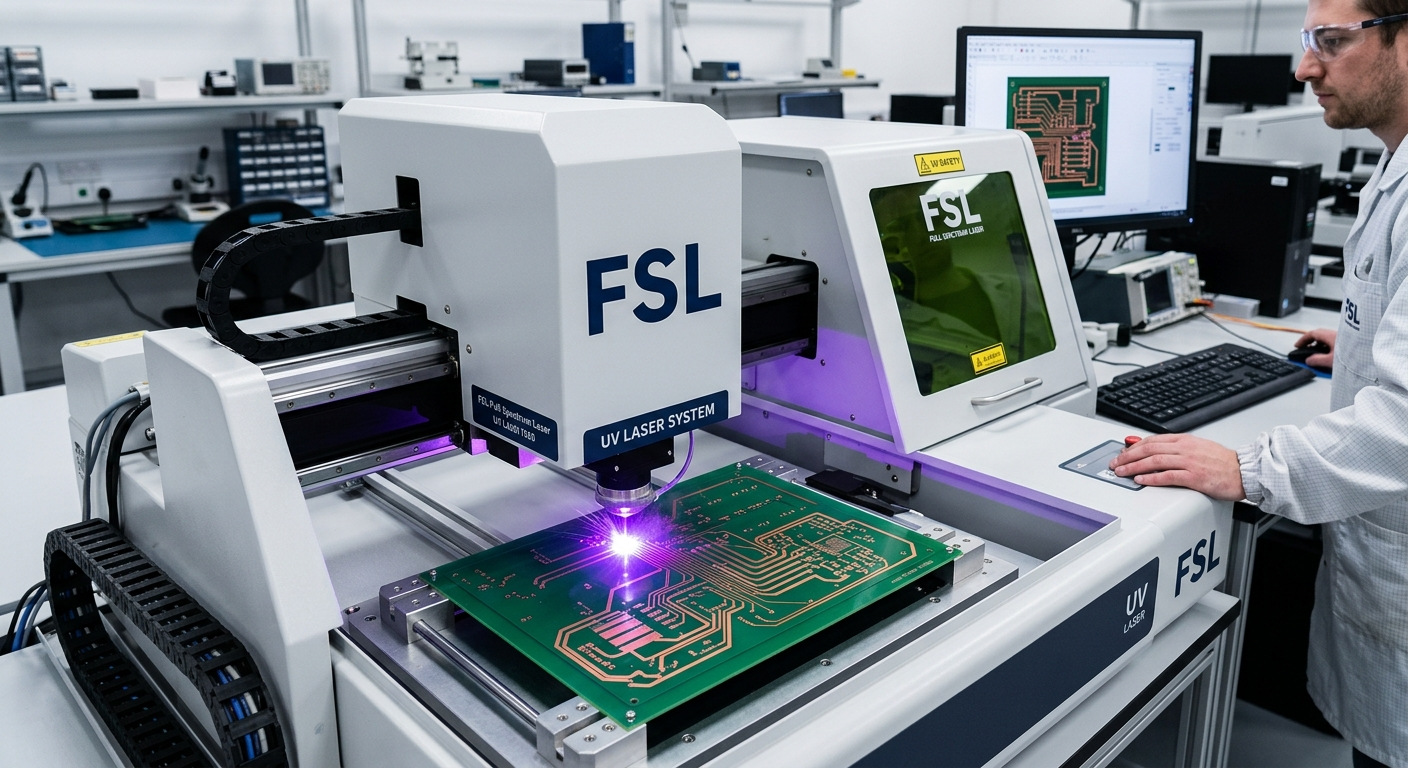
Instant Double-Sided PCBs with UV Laser + RE5: No Chemicals, No Mess
Prototyping circuit boards has traditionally meant either waiting days for a fab house or dealing with messy chemical etching that produces toxic waste. With Full Spectrum Laser's UV laser system and RE5 software, you can skip all of that and go from Gerber files to a finished double-sided PCB with drilled holes in minutes.
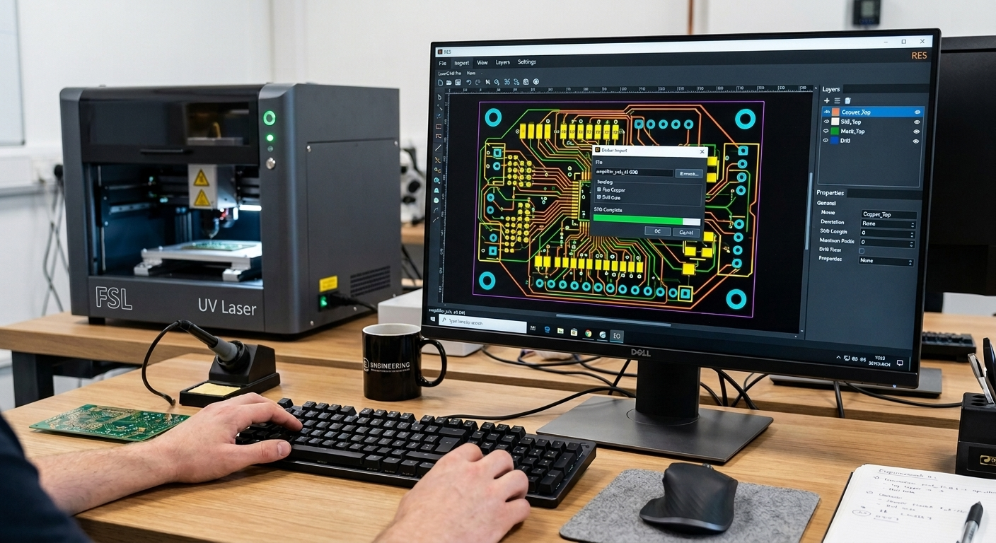
Direct Gerber Import
RE5 accepts standard Gerber files directly the same files you'd send to any PCB fabrication house. No conversion, no intermediate formats, no manual tracing. Import your design and RE5 automatically generates the laser toolpaths for:
- Path isolation The UV laser ablates copper between traces, creating clean electrical isolation without removing all the excess copper. This is faster and preserves more ground plane.
- Hole drilling Through-holes and vias are drilled directly by the laser with precise diameter control.
- Pad cleanup Pads and annular rings are cleaned and defined for soldering.
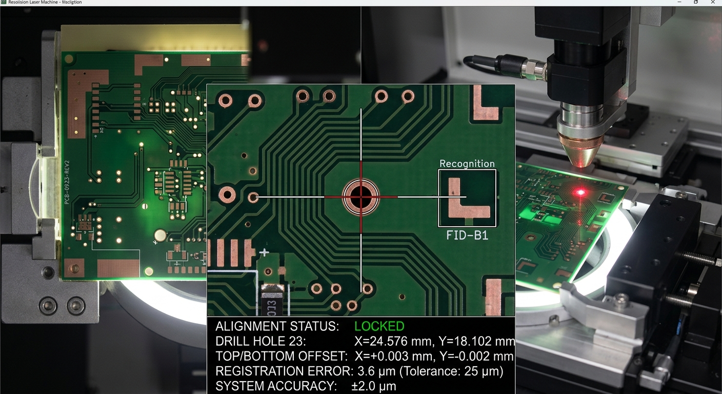
Camera Fiducial Alignment: Better Than 25µm
The real breakthrough for double-sided PCBs is RE5's camera-based fiducial alignment system. Here's how it works:
- Drill the through-holes first The laser drills all vias and mounting holes through the blank copper-clad board.
- Engrave the top side RE5 uses the drilled holes as fiducial reference points, then ablates the top-side trace isolation pattern.
- Flip the board Turn the PCB over.
- Camera auto-alignment RE5's vision system detects the drilled holes through the camera, automatically calculating the exact position and rotation of the flipped board.
- Engrave the bottom side The bottom artwork is precisely aligned and engraved, registering to better than 25 micrometers (0.001") with the top side.
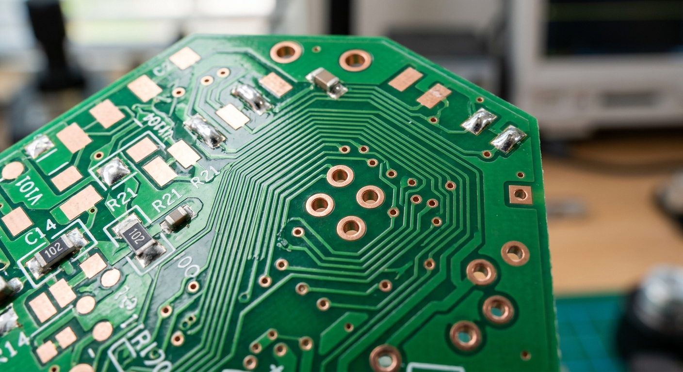
This level of precision means your vias line up perfectly, your SMD pads match between layers, and your board works the first time.
No Chemicals, No Mess, Instant Results
Traditional PCB prototyping with chemical etching involves:
- Ferric chloride or ammonium persulfate solutions
- Heating baths and timing
- Hazardous waste disposal
- Inconsistent results
- Separate drilling step with a CNC or manual drill press
With the UV laser approach, all of this is eliminated. The laser does both the trace isolation and hole drilling in a single setup. The process is completely dry no liquids, no chemicals, no waste. And since it's software-controlled, every board comes out identical.
See It In Action
Watch the full process from Gerber import to finished double-sided PCB:
Key Specifications
| Feature | Specification |
|---|---|
| Input Format | Standard Gerber (RS-274X) |
| Isolation Method | Direct path isolation (copper ablation) |
| Hole Drilling | Direct laser drilling |
| Layer Alignment | Camera fiducial, <25µm accuracy |
| Chemicals Required | None |
| Laser Type | UV (355nm) |
| Software | RE5 (RetinaEngrave 5) |
Did You Know?
You can also easily cut and separate tabbed PCBs with an FSL UV laser perfect for depaneling production boards without mechanical stress or dust. Contact FSL sales for more information.
Get Started
If you're prototyping electronics and tired of waiting for boards or dealing with chemical processes, an FSL UV laser with RE5 is the fastest path from design to working PCB. Explore our UV laser systems or contact our team for a demonstration.